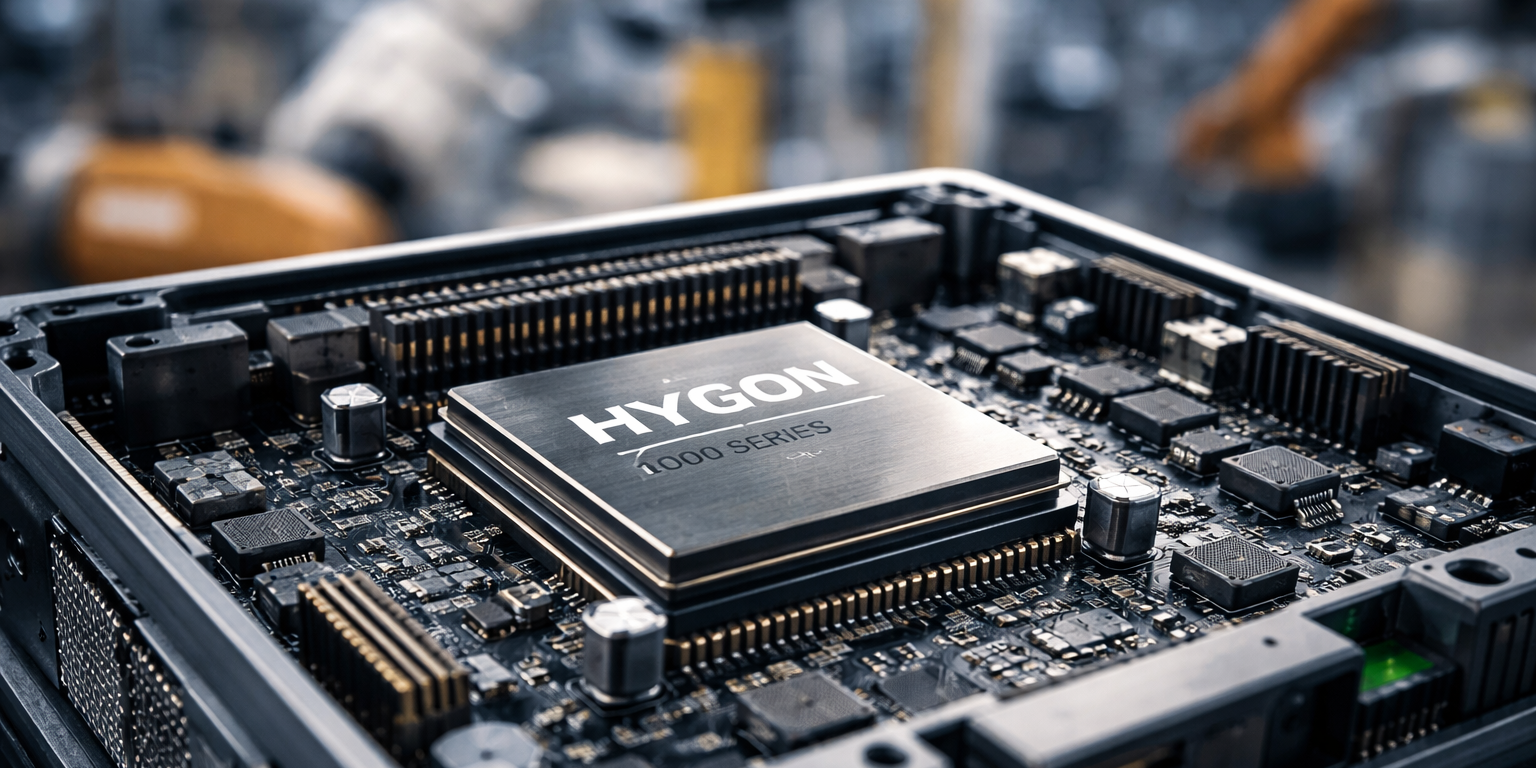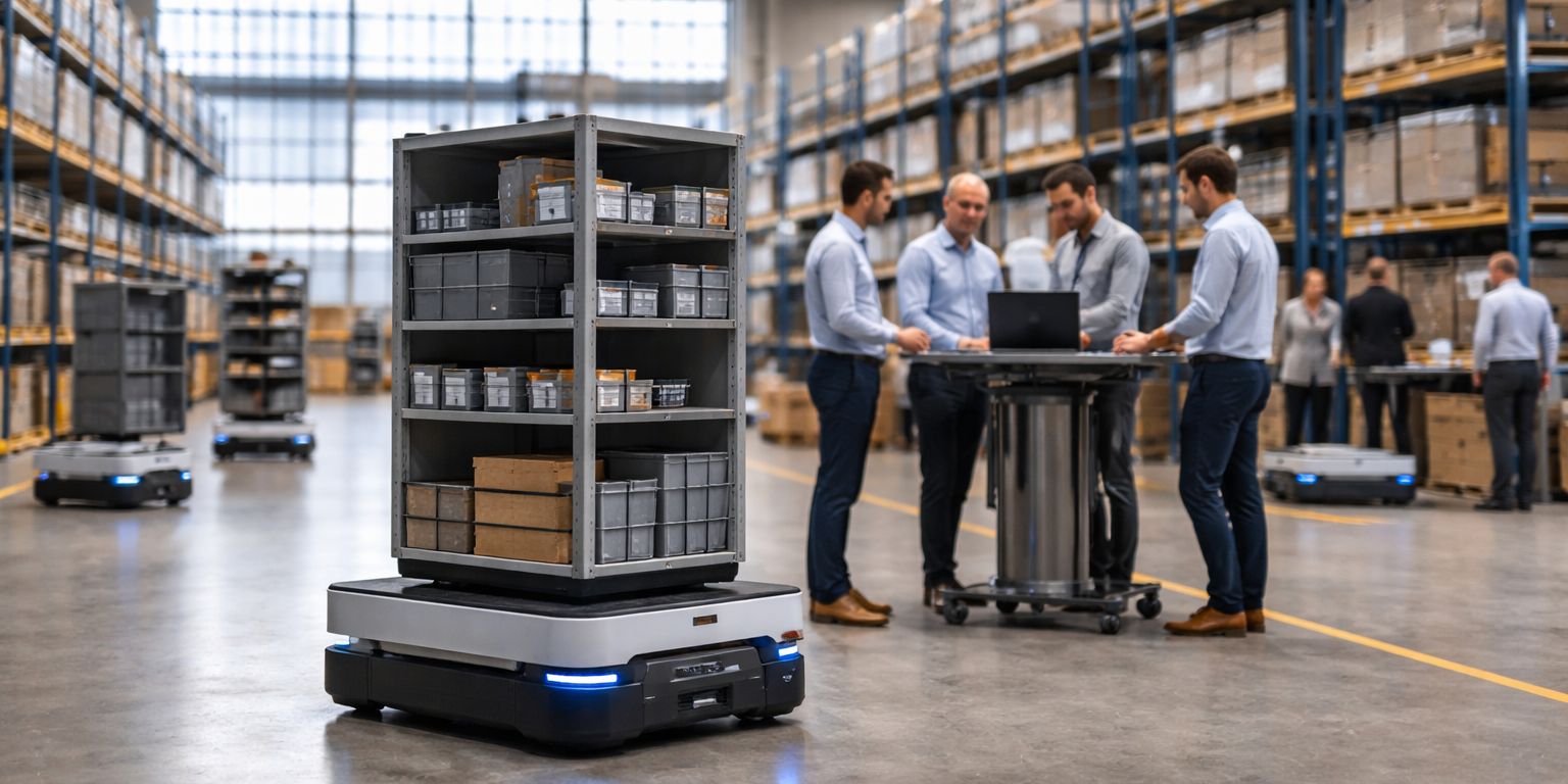

Samsung Electronics has partnered with Cadence Design Systems to develop a chiplet-based platform for physical AI semiconductors, aiming at robotics, autonomous vehicles, drones, and industrial automation applications, ETNews reported. The collaboration marks Samsung's foundry division pushing beyond traditional mobile and computing chips into specialized hardware that processes real-world sensor streams and controls mechanical systems. Unlike data center AI accelerators optimized for training large language models or running inference on static datasets, these chips prioritize low-latency sensor fusion, real-time decision-making, and precise motor control—the computational backbone of robots navigating warehouses, drones adjusting flight paths, and autonomous vehicles interpreting lidar feeds. Samsung has not disclosed launch timelines, lead customers, or pricing, but the Cadence partnership signals the platform will support heterogeneous integration, mixing different semiconductor process nodes and intellectual property blocks within a single package.
Chiplet architectures have gained traction as semiconductor companies confront rising costs and complexity in monolithic chip designs. Instead of etching every component—AI accelerators, sensor interfaces, motor controllers, communication modules—onto one massive die, chiplet platforms allow manufacturers to fabricate specialized units separately, then assemble them in a package using advanced interconnect technologies. This approach cuts development expenses, improves yields by isolating defects to smaller dies, and enables customization for different robotic systems without full chip redesigns. AMD popularized chiplets in consumer processors, while Intel has invested heavily in its Foveros 3D packaging. Samsung's entry with a platform explicitly targeting physical AI suggests the company sees robotics and edge autonomy as growth vectors distinct from its existing foundry customers in mobile and high-performance computing. The foundry business has lagged TSMC, capturing approximately 13% of the global market compared to TSMC's 60%, according to industry analysts. Automotive and industrial customers represent potential revenue streams less dominated by TSMC's established relationships.
Robotics companies currently cobble together processing architectures from general-purpose CPUs, field-programmable gate arrays for flexibility, and application-specific integrated circuits for power efficiency—a fragmented strategy that inflates bill-of-materials costs, complicates supply chains, and extends development cycles. A standardized chiplet platform could compress time-to-market for new robotic products if Samsung delivers competitive pricing, reliable yields, and integration tools that work across different process nodes. Cadence's involvement matters here: the electronic design automation vendor provides simulation, verification, and packaging design software used across the semiconductor industry. Their participation suggests Samsung intends to offer not just silicon manufacturing but a complete design ecosystem, reducing friction for robotics firms lacking deep chip design expertise. Physical AI chips must handle sensor data arriving at rates measured in kilohertz or megahertz—camera frames at 60 Hz, lidar point clouds at 10 Hz, inertial measurement units at 1 kHz—while issuing motor commands with latencies under 10 milliseconds. This differs fundamentally from cloud AI workloads, where milliseconds or seconds of latency often prove acceptable and power budgets stretch into hundreds of watts.
The foundry initiative puts Samsung in direct competition with Intel, which has positioned its edge AI accelerators and foundry services for autonomous systems, and TSMC, which supplies automotive-grade chips for companies including Tesla, Nvidia, and Mobileye. Intel's acquisition of Habana Labs and development of its Movidius vision processing units demonstrate similar ambitions in physical AI, though Intel has struggled to gain foundry customers outside its own product lines. TSMC maintains automotive partnerships and recently expanded capacity for 5-nanometer and 7-nanometer nodes suited to power-constrained edge applications. Samsung's differentiation likely hinges on packaging capabilities—the company has invested in 2.5D interposers and through-silicon vias for chiplet interconnects—and willingness to work with mid-tier robotics firms that lack the purchase volumes to command TSMC's attention. Whether Samsung can translate manufacturing expertise into design wins depends on execution: delivering promised performance benchmarks, maintaining quality across high-mix low-volume orders, and supporting customers through the integration challenges inherent in chiplet systems. The robotics semiconductor market remains fragmented, with no dominant platform comparable to Nvidia's position in data center AI, creating an opening for foundries that can offer compelling economics and rapid iteration.
What to Watch: Samsung's disclosure of lead customers or pilot programs will signal whether the chiplet platform has gained traction beyond concept development. Cadence typically announces customer deployments within six to nine months of platform availability, so watch for case studies or reference designs in upcoming quarters. Competitive responses from TSMC and Intel, particularly pricing or packaging announcements targeting robotics applications, will indicate whether Samsung's move pressures incumbent strategies. Any partnerships Samsung announces with robotics software frameworks or middleware providers—such as ROS, Isaac, or industrial automation platforms—would suggest efforts to reduce integration barriers for end customers.